
Improving Mazzilli's Driver
Better gate drive circuitry for the classic ZVS flyback converter
If you’ve ever delved into the world of high voltage power supply circuitry, you will have come across a classic flyback driver design attributed to Vladimiro Mazzilli. It’s simple, relatively robust and scalable to very high power levels.
For all its elegance, there has been one part of the design that I’ve always considered brutish — the gate drive circuitry. The feedback diodes, the zener clamps and the low value pull-up resistors are slow and inefficient. In a recent ElectroBOOM video, Medhi made a comment to this effect and asked the community if there were any solutions. Fortunately, there are some very basic modifications that can be made which massively improve the gate drive of this common circuit.
The Original
I haven’t managed to find the exact provenance of the circuit, but it almost certainly took inspiration from the Royer oscillator and/or the Baxandall converter. The schematic I have seen quoted as the original is below. The oldest copy I could find was from Tesla Downunder who claimed to have built it in 2004.
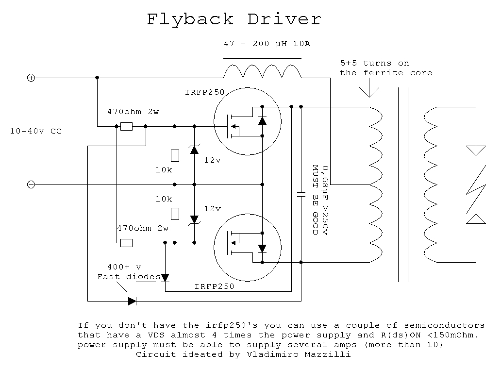
I’ve recaptured the schematic in LTSpice to run some simulations. I chose some components that differ from the originals and made a few educated guesses for the values that were unspecified, but this simulation should be fairly faithful to the original design. Because I’m only interested in the gate drive portion of the circuitry, I’ve omitted the secondary side of the transformer, meaning the circuitry is running fully unloaded.
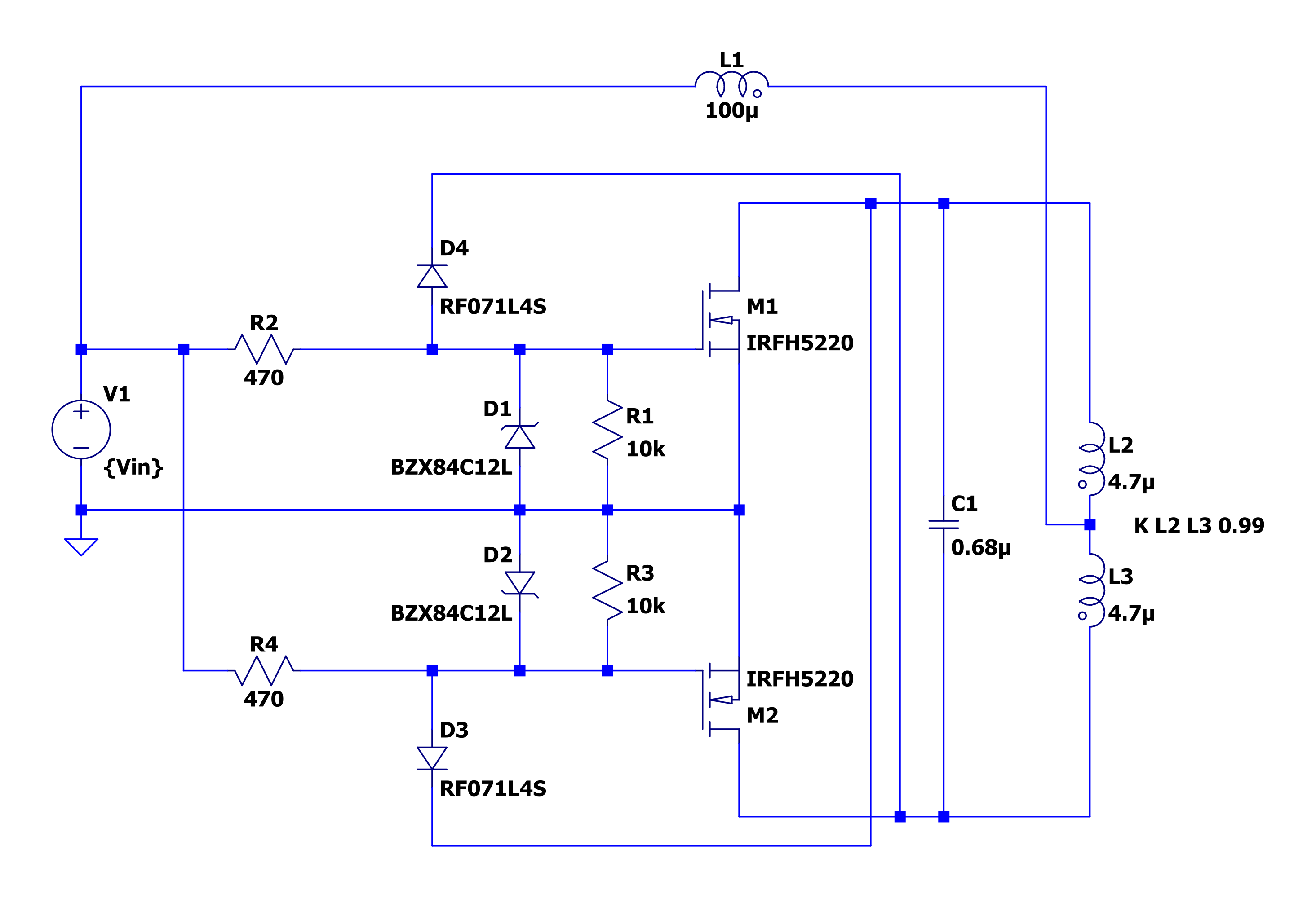
To turn on a FET (let’s choose M1), the 470 Ω resistor (R2) begins to pull its gate toward the supply voltage. When the M1 gate voltage hits the D1 zener breakdown voltage, the zener begins to conduct, clamping the gate voltage. This process has two problems:
- R2 limits the gate drive current. FETs with high gate capacitances combined with low supply voltages can result in slow turn on times. The FET spends more time than necessary in the ohmic region, resulting in higher losses.
- If the supply voltage is high enough for D1 to conduct, the full supply voltage is dropped across R2 and D1 while the FET is on. This results in excessive power loss in both R2 and D1.
We end up with a compromise. R2 needs to be small enough to ensure rapid switching, but large enough so there isn’t excessive power dissipation.
To turn off a FET (we’ll use M1 again), the coil L3 is fed back to the gate via a diode (D4). When the voltage at L3 drops to 0.7 V below the gate voltage, D4 begins to conduct and pull the gate low. This is an effective way to turn off the FET, but it has a problem. With the gate pulled close to ground, the full supply voltage is dropped across R2, resulting in excessive power loss.
Ultimately, when the FET is on, the full supply voltage is dropped across R2 and D1. When the FET is off, the full supply voltage is dropped across R2 and D4. This can be easily improved with a few minor modifications, resulting in better switching performance and lower losses.
The Update
The basic premise behind the improved gate drive is to feed back the signal from the opposing coil to drive the gates both high and low. We also need to clip the drive voltage to a safe level for the FETs. To achieve this:
- Create a local voltage reference a few volts above the required power FET gate voltage. I used a basic zener based voltage reference, but you can get fancier if you’d like.
- Pick two NMOS FETs with low gate-source threshold voltages (< 2 V), high drain-source voltage ratings (> 200 V) and low capacitances. On resistance doesn’t matter too much.
- Connect the gates of these two FETs to the voltage reference.
- Feed the signal from opposing coils through these FETs to the gates of the power FETs.
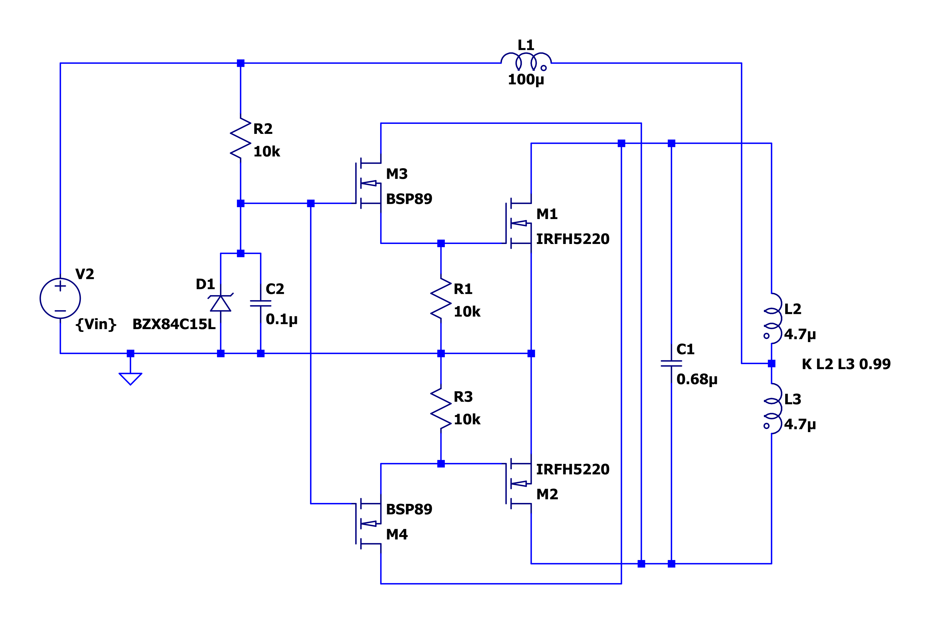
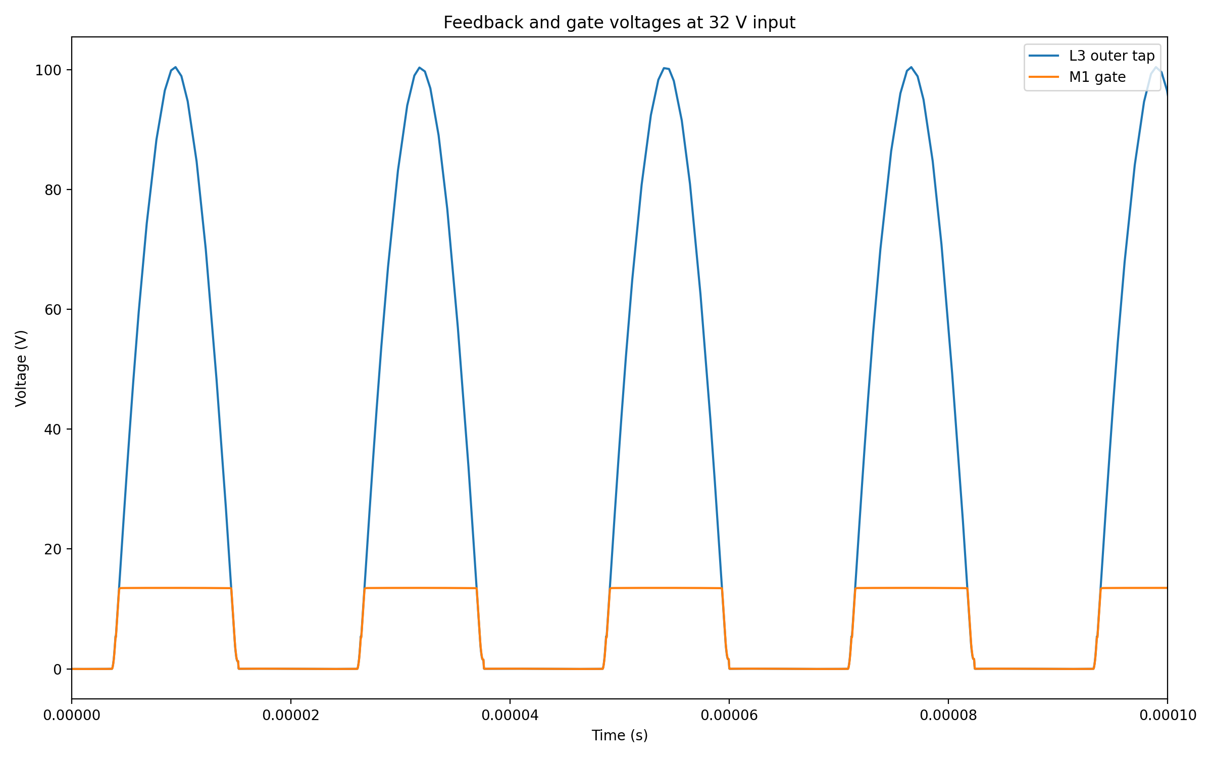
What we end up with at the gate of the power FETs is a clipped sine wave. The feedback is a very low impedance source, so it is possible to drive big MOSFETs with large gate capacitances. Unfortunately the rise/fall times are limited by the the fact that the drive signal is still based on a sinusoidal signal, but it still seems sufficiently fast.
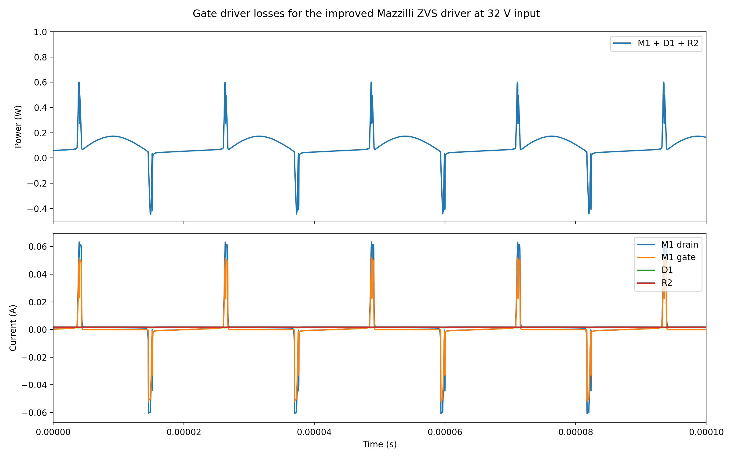
Besides charging/discharging the gate, not much current flows through the two added MOSFETs. The simple voltage regulator formed by R2 and D1 continuously draws a few mA, but it is substantially less than the pull up resistors in the old design.
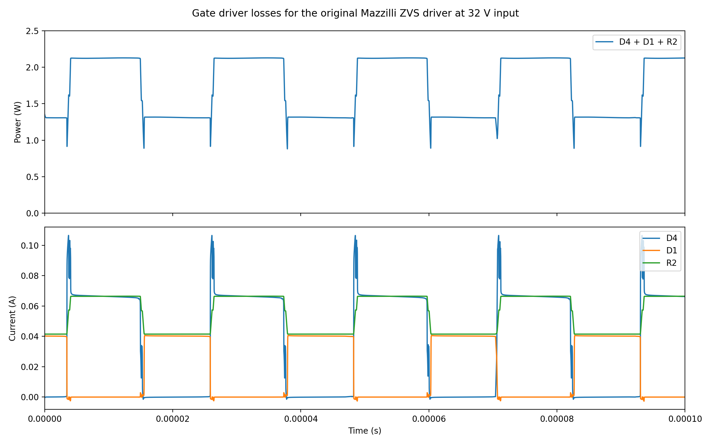
The Comparison
For a direct comparison, I ran simulations of the gate drive circuitry for a supply voltage range of 10 V to 40 V, which is the range the original flyback converter was specified over. The results speak for themselves.
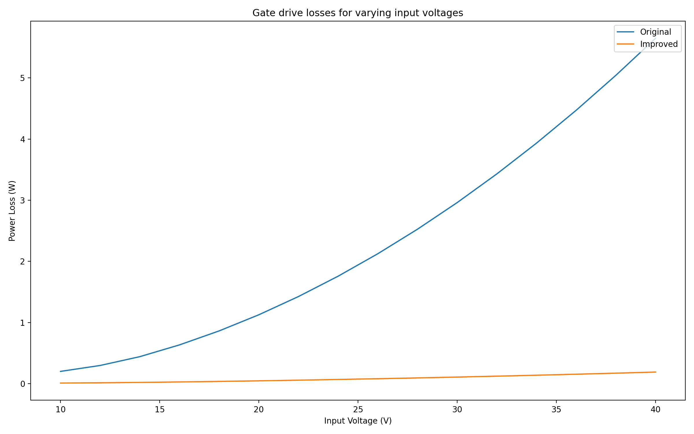
Not only is the improved gate drive much more efficient, it scales much better with input voltage. Losses only increase slightly as the input voltage is raised. In fact, so long as you can generate a clipping reference voltage and find FETs with sufficiently high voltage ratings, there is no reason this circuit couldn’t be used well above the rating of the original Mazzilli driver.
The Conclusion
I’ve used the improved gate drive circuitry in a photomultiplier tube power supply. Whilst it wasn’t a high power design, the supply was battery powered and therefore demanded efficiency. The need to reduce losses led to the aforementioned modification. I should note that this solution has been independently developed by others. After a quick search, I found this example of an uncannily similar design.
The original Mazzilli flyback driver is very elegant. It self resonates, it has inherent zero voltage switching, it provides an intrinsic boost of the input voltage and it only uses a handful of components. Still, it turns out you can make it even better.